|
||
|
|
|||||||||||||||
Table of contents |
||||||||||||||||
|
||||||||||||||||
| Contents | Next-> | ||||||||||||||||
|
||||||||||||||||
|
|
|||||||
| Meet Your Directors |
||||||||
|
Ever since my first encounter with electricity at age six, sparked by sticking something into the wall receptacle with its resulting flash of brilliance, all things electric, electronic and magnetic have captivated my interest. By fourth grade I had a shoebox of batteries, switches, wire and light bulbs to tinker with after finishing my school assignments. Fast forward to high school in my last year I traded my slide rule and $1106.59 (today's dollars) for a 'used' HP programmable calculator. University saw computer input change from punch cards to terminals connected to the time-shared mainframe housed in its own building on campus. At my first job designing transformers the goals were the same as today, make the smallest, lowest cost (60 Hz) transformer or inductor possible for the application. The tools evolved from calculator to teletype terminal to personal computers with ever more capable hardware/software. Switch mode power supplies came of age and quite literally transformed the industry. The advancement of active and passive components continues to this day with ever increasing application in our electrified digital world. A lot has changed over 45 years and the PSMA has been there through it all. Having the privilege to serve as a director on the PSMA board and as a co-chair on the Magnetics Committee over the past several years has been a rewarding experience. I have met many great people. I would encourage all young people in the industry to join in and get involved. Networking with colleagues from across the industry broadens your perspective and gives you an appreciation of their challenges and contributions to your work. Working together, both corporate and academic institutions are advancing power electronics to new levels. The PSMA brings these various components together to serve all who are involved in power electronics. |
||||||||
|
|
|||||||||
APEC 2025 News |
||||||||||
|
APEC Turns 40 in Atlanta, March 16-20. Come and be Part
Here's a quick rundown of the key APEC events:
As a PSMA member, you and your company collages are eligible for very attractive Full conference discounts APEC - The Premier Event in Applied Power Electronics™
|
||||||||||
|
|
|||||||
2025 Annual Meeting to be Held in Atlanta |
||||||||
|
Members and guests are also invited to remain for the Board of Directors meeting that will immediately follow the Annual Meeting. Participation in these meetings will provide you with the opportunity to network with colleagues from other companies and to influence the direction of the PSMA and the power sources industry. Be sure to visit us at the PSMA booth, in the APEC hub of the exhibition area during APEC. PSMA is again sponsoring the popular PSMA/ APEC Passport Program in the Exhibit Hall. Visit the booths of participating PSMA members to enter your name into a raffle drawing.
|
||||||||
|
|
||||||||
PSMA Magnetics Committee and PELS TC2 High Frequency |
|||||||||
Power Magnetics @ High Frequency
The purpose and focus of the workshop are to identify the latest improvements in magnetic materials, coil (winding) design, construction and fabrication, evaluation and characterization techniques and modelling and simulation tools. The Workshop will target the advancements deemed necessary for power magnetics to meet the technical expectations and requirements of new and evolving market applications. These are driven by higher operating frequencies and emerging topologies together with continuous advances in circuits topologies and semiconductor devices. The target audiences for the 2025 Power Magnetics @ High Frequency Workshop include the designers of power magnetic components for use in electronic power converters, those who are responsible to implement the most technologically advanced power magnetic components necessary to achieve higher power densities, specific physical aspect ratios such as low profile, higher power efficiencies and improved thermal performance. The target audiences also include people involved in the supply chain for the power magnetics industry ranging from manufacturers of magnetic materials and structures, fabricators of magnetic components, providers of modelling and simulation software as well as manufacturers of test and characterization equipment. The theme of the 2025 Power Magnetics @ High Frequency will be integrated magnetics, defined as magnetic structures that perform two or more functions. The morning technical session will feature a keynote presentation and four lecture style presentations concluding with two panel Q&A sessions. There will be a five-minute Q&A after each lecture presentation. The schedule for this session is:
The technical capabilities and disciplines that will be demonstrated and displayed during the technology demonstration/poster sessions are as follows:
The third technical session will feature a keynote presentation and three lecture style presentations concluding with a panel Q&A session. A five-minute Q&A. will follow each presentation. After all presenters have presented, all the presenters will reassemble for a twenty-minute panel Q&A The schedule for this session is as follows:
There will be a networking hour after the afternoon technical presentation session has completed. This will be the last opportunity to interact with the technology demonstration presenters and the student poster presenters as well as an opportunity to relax and have informal dialogues with other workshop attendees. Registration for the workshop is limited and is open at the following URL: https://psma.com/power-magnetics-high-frequency-workshop-2025-registration The agenda for the 2025 Power Magnetics @ High Frequency is available on the PSMA website at the following URL: https://psma.com/2025_Power_Magnetics_at_High_Frequency_Agenda
|
|||||||||
|
|
||||||||
Registration is Open for |
|||||||||
|
EVENT OVERVIEW
IWIPP 2025 will be held April 8th-10th, 2025, on the beautiful campus of the University of Alabama, Tuscaloosa, USA. IWIPP 2025 will feature keynote talks from distinguished experts in the packaging field, a broad range of technical sessions, and many networking opportunities, all of which are included in the registration fee. ONLINE REGISTRATION AVAILABLE PRELIMINARY PROGRAM PUBLISHED REASONABLE REGISTRATION FEES Best regards, Sponsored by: IEEE Power Electronics Society (PELS)
|
|||||||||
|
|||||||||||||||||||||||||||||||||||||||
Snapback TVSs Deliver More Accurate and Robust |
|||||||||||||||||||||||||||||||||||||||
|
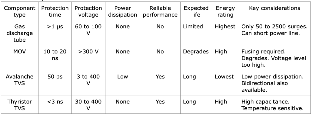
This article begins with some comments on the technology and market trends that are driving adoption of TVSs. It then provides an overview of conventional TVS devices, discussing their pros and cons, starting with historical solutions like SCRs, and then moving onto the currently used gas discharge tubes, metal oxide varistors, and TVSs. With that as background, the article describes how snapback TVS device technology offers a groundbreaking approach to circuit protection compared to previous TVS methods and devices. The characteristics and behavior of snapback TVSs are discussed with some data presented to illustrate the differences between conventional and snapback TVSs. This leads to a discussion of application benefits and an application example. The Growing Need For TVS Protection First, some history on transient voltage suppression is needed. The real world is replete with both natural and manmade transient electrical energy. In the beginning, most electronics didn't really need much protection from these events, but when electronics applications transitioned from solid-state to integrated-circuit—and now to VLSI—technologies, each generation became more sensitive to transients and surges. Circuit protection became increasingly necessary on ac and dc power lines and on the I/O connectivity that makes equipment work in the real world. Lighting applications, for example, until a short time ago were 100% electric and employed electronics based on magnetics and capacitors for their ballast designs. Then the lighting industry moved to using more complex and sensitive electronics, from high-frequency switching electronic ballasts for fluorescent lighting, to the now ubiquitous LED lighting systems that use electronic drivers. Today, proximate lightning and utility equipment switching events cause plenty of transients that can damage lighting electronics. Add to this challenge that manufacturers often require warranties of five, seven, and even 10 years—despite these electronics being more susceptible to damage. Along with the challenge of protecting more-sensitive electronic systems, electronics designers must conduct industry qualification testing and meet a number of specifications for many applications worldwide. These include IEC61000-4-2/3/4/5 and the IEEE C62.41 ringing waveform testing, as well as tests for automotive such as ISO and SAE specifications ISO7637-2 or ISO16750-2. Evolving TVS Technology Before describing snapback TVS technology, let's explore the historical approaches to mitigating electrical transients. The purpose of a TVS device is to convert transient electrical energy into transient thermal energy and to dissipate it as heat. One of its primary goals is to dissipate this heat energy as quickly as possible and then reset for another event. One of the first TVS solutions was the SCR clamp. Although it worked, this device was very prone to false triggering. Proximate noise, either conducted or radiated, entering the circuit triggered the SCR until the power source was recycled and the current through the SCR went to zero. This was not an option for equipment needing 100% uptime and, for that reason, SCR clamps aren't really used today. Another early technology, gas discharge tubes, or GDTs, were mainly used as circuit protection in the era of copper telecommunications lines to protect against lightning strikes. They are still widely used in a plethora of applications, often in combination with other protection devices. Among other benefits, GDTs are reasonably fast-responding. However, they have a limited lifetime and degrade with repeated application of transients depending on the magnitude of the transient. In the 70s, we saw the invention of the MOV (metal oxide varistor). This device was a significant step forward in TVS technology, offering many benefits and few downsides. However, both MOVs and gas tubes can fail short and thus require the addition of series current-limiting devices like fuses and circuit breakers. From the late 70s to the mid-80s, semiconductor TVS devices were developed, and were available in both bi- and uni-directional options. Semiconductor TVS device have fast response times and good thermal performance with a lifespan that can be limited by simply not overdissipating (overheating) the die too far above 175°C. They are more precise and rugged than previous methods—unless they are overdissipated. Table 1 compares the characteristics of the traditional TVS devices described above. All of these technologies have drawbacks in precision, accuracy, and temperature coefficient. For example, MOVs are not able to withstand multiple transient events. I have seen MOVs turned into talcum powder with a couple of leads sticking out of the board as a result of too much repetitive transient energy being applied. In addition, all types have a tempco issue in which the clamping voltage tends to change with temperature. It's not only the ambient temperature that's a concern in this regard but also the repetitive pulses that can heat up the protection device. This behavior is a problem since, as stated earlier, a key function of a TVS device is to dissipate the heat from the transient being converted into thermal energy.
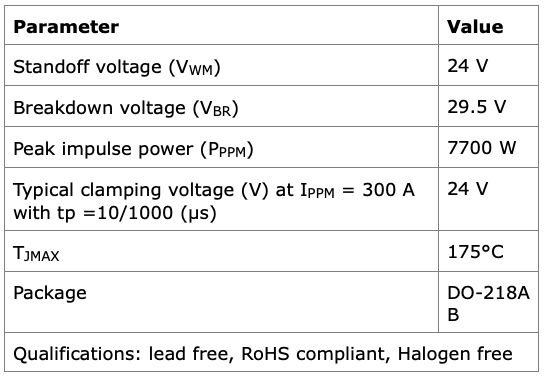
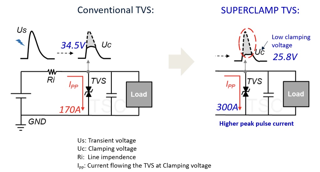
Emergence Of Snapback TVS Technology Ideally, a TVS device would have a "not to exceed" voltage, such that a 24-V bus could be protected with a 24- V protection device. It would also have zero response time, infinite ability to withstand repeated transients of any magnitude, no degradation with application of repeated transients, good reliability and long life, a high-energy rating, and the ability to fail-safe. Finally, the device would not allow applied transients to exceed the protection voltage—regardless of the device temperature. In recent years, the introduction of snapback TVS technology by semiconductor companies[1-5] has provided an evolution in transient voltage suppression that brings us closer to this ideal. Unlike traditional TVS diodes, which clamp the voltage at a certain threshold during a surge, the snapback TVS device provides a unique behavior where its clamping voltage drops to a significantly lower "snapback" level once the device begins conducting. Achieved through advanced semiconductor engineering, this capability ensures better protection for low-voltage components and minimizes the stress on the protected circuitry. And offering a much better clamping ratio than conventional TVS devices, snapback technology provides both clamping and self-resetting characteristics. In contrast, conventional TVSs act more like power Zener diodes. Snapback TVS devices, whose working principle is rooted in their silicon-based design, react almost instantaneously to transient events. This rapid response ensures that sensitive circuits are shielded from harmful voltage spikes before they can be damaged. The response time is faster than alternative options (see "Protection time" in the table above) and the ability to withstand repetitive transients is limited only by the device's die temperature—unlike MOVs and GDTs with their wearout mechanisms. Fig. 1 shows the key parameters of a Taiwan Semiconductor SUPER CLAMP device. This 7700-W, 24-V surface-mount snapback TVS device (model LTD7S24CAH)[5] offers better accuracy and precision than previous semiconductor TVS protection devices. It can pass AEC-Q automotive reliability standards even when used in extremely demanding applications. Snapback TVS technology provides powerful protection in a small form factor, making it suitable for integration into space-constrained designs. As a low-clamping TVS with snapback characteristics, the LTD7S24CAH provides an extremely low clamping ratio between working voltage (VWM) and clamping voltage (VC). The low clamping ratio TVS can suppress high surge current to provide lower clamping voltage than conventional TVS and MOV devices (Fig. 2).
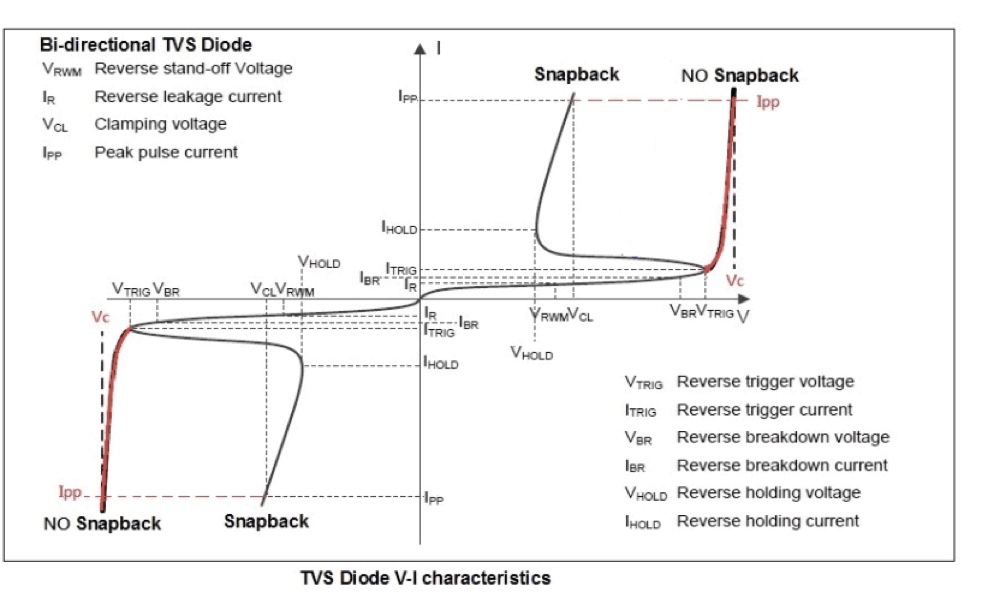
Despite their compact size, snapback TVS devices can handle substantial surge currents, offering robust protection against manmade or naturally occurring high-energy transients. Fig. 3 shows the behavior distinguishing a snapback TVS device from a conventional bidirectional TVS diode. When a transient voltage surge occurs, the device clamps the voltage to a predetermined threshold. As the current increases, the device enters a "snapback region" where the voltage decreases to a lower, more stable level to provide enhanced protection. As the current approaches zero, the snapback TVS device returns to a high impedance state, resetting for the next transient application.
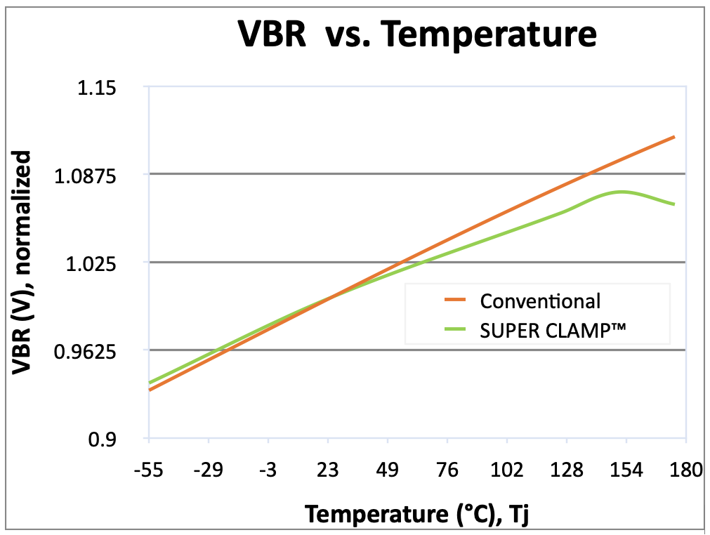
Because it has a "not to exceed" limit capability, the snapback TVS device obviates the need to overdesign. It allows designers to use lower working voltage components, such as capacitors, switching MOSFETs, reverse polarity protection diodes, and regulators. Additionally, its breakdown voltage (VBR) varies much less over temperature than conventional TVS devices (Fig. 4). This VBR stability vs. temperature helps the designer anticipate voltage range over temperature considerations (i.e., what could happen when…)
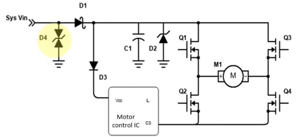
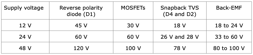
Application Benefits As electronics applications of every form continue to shrink in size, the need to meet the requirements of regulatory compliance for EMI qualification, which include transient protection, makes snapback technology a compelling approach. By reducing the voltage excursion during a surge, snapback TVS devices minimize power dissipation across the protected components, preventing damage and increasing system reliability. Eliminating the need for overdesigning, they can enhance design size and weight goals, while passing the qualification testing and increasing survivability in the application. Many electronics markets can benefit from using snapback TVS protection devices, from automotive (HEV 48-V buses, alternators) and telecom/datacom/networking and EMP protection systems, to industrial process controls, avionics, battery management systems and chargers—any protection application working at 24 V or greater. Snapback TVS technology is particularly beneficial in applications with low-voltage electronics. Its ability to return—or snap back—to a lower voltage during a surge significantly reduces the risk of overvoltage damage to downstream devices, making it very desirable for use in modern electronics that have shrinking voltage margins. The snapback TVS device can be combined with other protection methods to allow the circuit to keep working in many electrically and environmentally hostile applications. The snapback TVS technology also helps protect automotive electronics challenged by stringent reliability qualifications and cost pressures. The devices can be used in designs to help pass stringent AEC-Q testing and to survive harsh environments encountered in ICE (internal combustion engine), HEV and full electric vehicles by protecting bus voltages and the application of charging current. Additionally, snapback technology is well suited for use in industrial equipment, sensors, medical, and process automation systems that must work 24 x 7. In applications, such as factory automation equipment, that must operate reliably in harsh environments where repetitive transients are common, snapback TVS devices are not only more precise, they can also sustain multiple transient fault events and still survive, unlike MOVs and GDTs. Snapback TVS technology is also instrumental in protecting sensitive communication circuits from transients, including 5G base stations, telecom and networking systems, data transmission lines and other I/Os. Furthermore, it is essential where protection must be validated such as through UL recognition of protection devices used in the application. Additionally, snapback TVS technology allows lighting applications to meet reliability standards by surviving and continuing to operate in applications where lightning strikes and line transients are frequent occurrences. This capability is highly beneficial in a market typified by long warranties and connections to the ac mains. One caveat in the application of snapback TVSs is that there is the potential for latchup if the clamping voltage selected is below the working voltage. Application Example: BLDC Fan Speed Controller Fig. 5 illustrates how snapback TVS devices offer advantages over conventional TVS approaches when protecting a single-bridge BLDC (brushless direct current) fan speed controller. In this application example, the low VC of the snapback TVS device helps protect the motor controller and other components with lower voltage stress. Compared with using a conventional TVS or other alternatives, it also has greater power density and results in less overdesign. Table 2 lists the ratings of devices that would be applied at different supply voltages and assumes use of a snapback TVS for both D4 and D2. Consider the case described for the 24-V supply voltage. In this case the clamping voltage of the snapback TVS is just 26 V for D4, whereas in the case of a conventional TVS it would typically be 35 V.
Conclusion Its unique ability to combine low clamping voltage with robust surge-handling capacity positions the snapback TVS device as an essential component in modern electronic designs. Whether in consumer gadgets, industrial machinery or automotive systems, snapback TVS devices are set to play a crucial role in ensuring the safety and reliability of next-generation electronics of all types. As electronic devices become more sophisticated and sensitive due to VLSI geometry reductions and other low-voltage IC methods, the demand for this advanced circuit protection technology will continue to grow. Research and development in this field are likely to focus on further reducing clamping voltage, increasing surge-handling capability, and enhancing integration into multi-functional protective components. References 1. XClampR TVS, Diodes and Rectifiers - TVS Protection page, Vishay website. About The Author Kevin Parmenter is an IEEE Senior Member and has over 35 years of experience in the electronics and semiconductor industry. Kevin is currently director of Field Applications Engineering North America for Taiwan Semiconductor. Previously he was vice president of applications engineering in the U.S.A. for Excelsys, an Advanced Energy company; director of Advanced Technical Marketing for Digital Power Products at Exar; and led global product applications engineering and new product definition for Freescale Semiconductors AMPD - Analog, Mixed Signal and Power Division. Prior to that, Kevin worked for Fairchild Semiconductor in the Americas as senior director of field applications engineering and held various technical and management positions with increasing responsibility at ON Semiconductor and in the Motorola Semiconductor Products Sector. Kevin also led an applications engineering team for the start-up Primarion. Kevin serves on the board of directors of the PSMA (Power Sources Manufacturers Association) and was the general chair of APEC 2009 (the IEEE Applied Power Electronics Conference.) Kevin has also had design engineering experience in the medical electronics and military electronics fields. He holds a BSEE from Purdue University and a BS in Business Administration from Colorado Technical University, is a member of the IEEE, and holds an Amateur Extra class FCC license (call sign KG5Q) as well as an FCC Commercial Radiotelephone License. For further reading on circuit protection in power electronics, see the "How2Power Design Guide," locate the Design area category and select "Power Protection".
This article originally appeared in the February issue of How2Power Today, available online at www.how2power.com/newsletters.
|
|||||||||||||||||||||||||||||||||||||||
|
||||||||||||||||
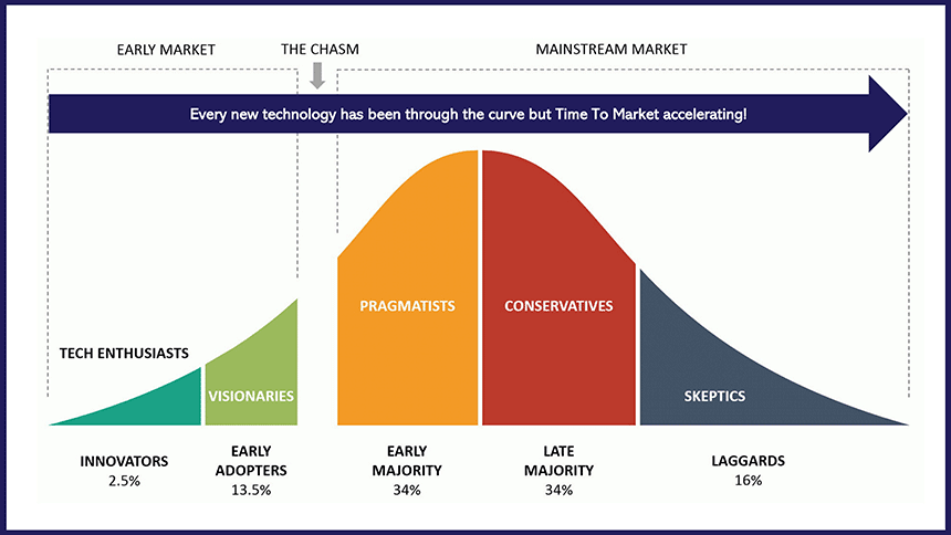
Crossing the chasm with success |
||||||||||||||||
|
The Early Adopters boosted GaN adoption!
Introduced in 2005, digital control in power supplies has been broadly adopted but after 20 years it is still considered by skeptics to be a curiosity. In normal circumstances it would have been the same for the adoption of WBG, but market demand for smaller, lower power consumption, industry modernization, emerging technologies and the famous Artificial Intelligence have contributed to the speed of the learning and implementation processes. As the Applied Power Electronics Conference (APEC) is celebrating its 40th anniversary, it is good to remind that for many technology analysts, the cornerstone of WBG took place at APEC-2018 when 'challengers' demonstrated the commercial potential of WBG technology. It is not possible to name all of them but among the leaders promoting GaN I would say that the Efficient Power Conversion's (EPC) idea to implement GaN in LiDAR was really interesting, especially with that technology becoming preponderant in the new generation of vehicles (Figure 02).
LiDAR, an acronym for "Light Detection And Ranging" is a technology that uses laser pulses to map out an environment. When the pulse contacts an object or obstacle, it reflects or bounces back to the LiDAR unit. The system then receives the pulse and calculates the distance between it and the object based on the elapsed time between emitting the pulse and receiving the return beam. LiDAR systems are capable of processing a high volume of pulses with some systems emitting millions of pulses per second. As the returning beams are processed, the system generates a comprehensive view of the surrounding environment, enabling the use of sophisticated computer algorithms to discern shapes and identify objects such as cars and people. Due to their high-frequency operation, which enables faster laser pulse modulation, LiDAR applications were part of the early adopter of the GaN technology. Their capacity to manage high-currents with minimal losses is paramount for enhancing accuracy and extending range in LiDAR systems. GaN's efficiency and power density advantages enable the development of smaller, lighter LiDAR systems, making it a suitable solution for various applications, including automotive, security, robotics, drones, and aerospace. Behind the scenes, the development of LiDAR applications has contributed to the adoption of GaN and is representing a significant volume. 2018 was also the year in which USB adapter manufacturers started to consider implementing WBG technology to offer more power in smaller packaging and to gain a competitive advantage. I mentioned EPC but Navitas Semiconductors is another example of an innovative company that in the early days pushed GaN integration to a higher level by packaging drivers and switches on the same substrate. Making Complex Simple – The Key to success!
When first presented, WBG power semiconductor utilization was limited by the number of drivers available, making it difficult for power designers to consider the technology. Also, new technologies are always questioned regarding reliability and sustainability. Market adoption depends on how simple it is for power designers used to conventional MOSFETs to use WBG, and semiconductor manufacturers' speed in developing 'ready-to-use' solutions that include driver, protection, monitoring and many other functionalities into a single chip. This not only simplifies implementation but also reduces the overall size of the power stage, and combined with higher switching frequencies make it possible to reduce the size of magnetics, thus increasing power density whilst reducing the overall volume and mass of the power supply. As mentioned, among the many products that could benefit from the implementation of WBG technology, we could pinpoint portable equipment chargers. As end-users we all expect USB chargers to deliver more power, to charge faster and to be smaller and lighter.
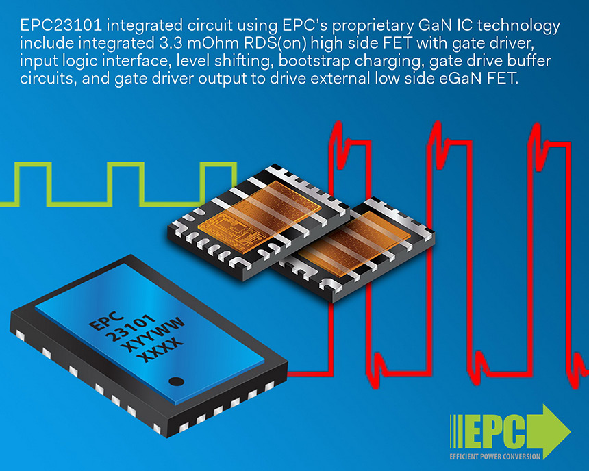
In 2020, this wish became a reality and one example of the benefit of using WBG GaN to achieve that is a 110W Mini fast charger that is over 12 times smaller than the 96W charger supplied with the Apple MacBook Pro 16 launched by OPPO (Figure 03). This has been made possible by combining the Navitas GaNFast power ICs with a planar transformer, an optimized topology and a higher switching frequency. At the same time, EPC released a GaN IC integrating everything to make it simple for power designers to implement into their new designs (Figure 04). Those examples illustrate how WBG GaN manufacturers rapidly moved from 'complex' to 'simple' to implement the technology, contributing to generate volume and market adoption. High power GaN setting-up a foundation for future! Presented examples addressed low and mid power applications but as well, WBG received high interest for high power applications such as Electric Vehicles (EV), renewable energy and many others. Electric Vehicles (EV) have seen a significant uptake of WBG technology and as of today it is the dominant technology in battery chargers, power trains and as already mentioned, equipment such as LiDAR. EV is often presented as the showcase for the adoption of WBG though less well-known is the role of Information and Communication Technology (ICT) in supporting research on GaN and SiC. This research aimed to develop the next generation of power supplies to support hyper-processors applications and data centers for Artificial Intelligence (AI). The rapid adoption of AI is accompanied by a significant growth in data volume and increased computing requirements. By 2025, the data volume is projected to reach 180 zettabytes, up from 15 zettabytes in 2015. According to OpenAI researchers Dario Amodei and Danny Hernandez, the amount of computing power used for deep learning to train state-of-the-art AI models has been doubling every 3.4 months since 2012. This continuous increase in computational power directly impacts electricity consumption, with AI data centers expected to account for up to 7% of global electricity demand by 2030.
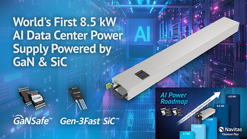
Optimizing energy utilization has always been a concern for the ICT manufacturers, requiring all suppliers, from infrastructure to components to reduce energy consumption. From the early days of research to improve the power supplies, AC/DC or DC/DC energy efficiency, power electronics designers explored new technologies and partnerships with semiconductors manufacturers. Several papers have been presented at APEC and other conferences. It's worth mentioning Navitas Semiconductors, who at APEC 2022 presented "Electrify Our World" introducing the benefits of WBG in ICT and, in 2024, the materialization of the utilization of that technology in power supplies for datacenters, where they predicted that power demand per unit will ultimately reach 10kW (Figure 05 insert). Exploring the optimum benefits of combining GaN and SiC, the company released a 8.5kW, 98% efficiency reference design, complying with the with Open Compute Project (OCP), Open Rack v3 (ORv3) specifications and ready for stringent energy efficiency standards (Figure 05). This is a good representation of what has been achieved when combining WBG and other advanced technologies to power today and tomorrow ICT applications and more to be expected. Industrial applications in transition mode. As presented by the market analysts, despite GaN having been on the market for several years the market remains fragmented with each GaN manufacturer offering different combinations of products and services addressing specific segments. To get the best out of GaN, power designers must work in close cooperation with semiconductor manufacturers and embrace one-stop solutions (GaN transistor, driver, protection, etc.) tightened to a single source, albeit raising concerns about the risks of using products from a new supplier with limited history and financial background. That, without mentioning some applications e.g., railway apps requiring 25 years lifetime and products availability for maintenance, requiring a solid and sustainable supply chain are part of complex equation when considering a new technology.
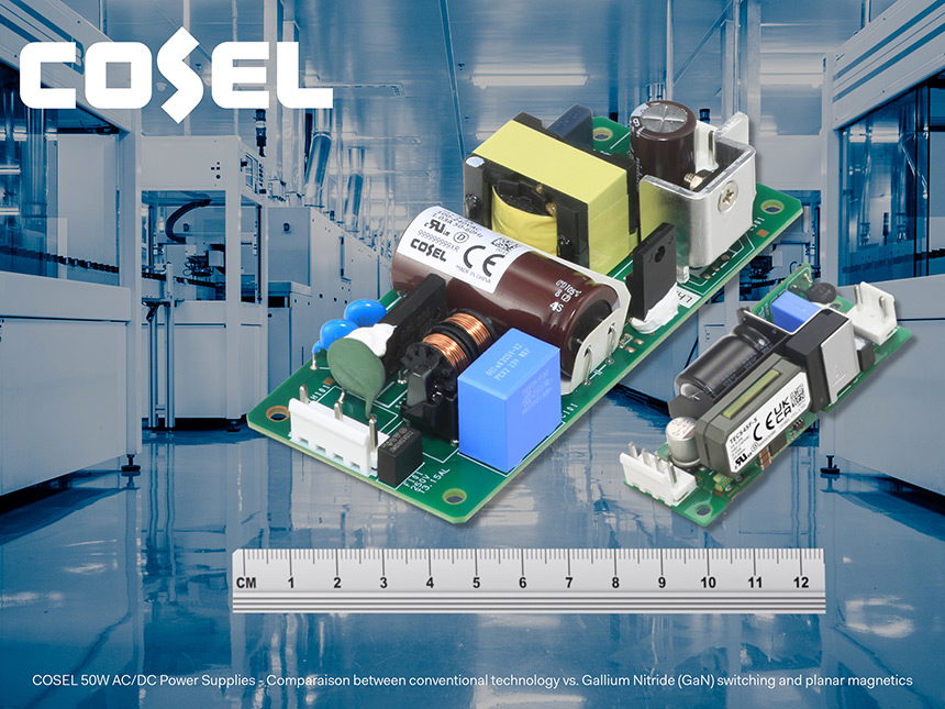
Due to that, the adoption in industrial, railway and medical applications may be slower than in EV, ICT and consumers but the obvious benefit of WBG motivated designers to explore that way. One example is the outcome from COSEL research to combine digital control, GaN and planar magnetics that makes it possible to offer very compact power solutions that are easy to integrate into small space environments (Figure 06). That will make it possible to house the power supply and a battery backup in the same volume as the conventional version of a similar power supply. As we are moving forwards to new applications requiring higher performances, WBG will gain market shares and follow the same path followed by the early adopters. Conclusion
|
||||||||||||||||
|
|
|||||||
PSMA Core Loss Database |
||||||||
|
I always defend that the world of Power Magnetics is quite behind other engineering sectors regarding software tools and data standardization. Sure we have tons of devices to characterize small signal parameters, like inductances or capacitances, but if we talk about real power large-signal characterization we don't have so many. And the ones we have are really expensive, which makes them affordable only to large companies, and they tend to keep their measurement data private due to competition. To change this situation, two parallel efforts are underway. The first is the development of a standard format for exchanging core data electronically. Members of the IEEE PELS ETTC are working on this by updating the existing IEEE 393 standard. The second effort is to make the exchange of data easy. To this end, the PSMA, through the Magnetics Committee has initiated a special project to create an open-source database, where everybody can upload their measure core loss, and everybody can read it and use it for free, including clean structured data about the magnetic and measurement setup used for each data point. And because this does not make too much sense without an affordable way of measuring the core loss, we are developing an open-source measurement equipment based on the Triple Pulse Test developed by Jun Wang at the University of Bristol And yes, that includes the schematic and layout of the boards, the firmware, the control software, and the connection to the public database. Interested in knowing how you can properly measure large-signal core losses in your laboratory? Do you want to collaborate in an open-source project that aims at fully characterizing magnetic components in an affordable way? We will be presenting at the PSMA workshop at APEC 2025 this year, come and visit us!"
|
||||||||
|
||||||||
IPC-9592C – A Call |
||||||||
|
Topics that may be included in the update are:
Additional topics will also be considered based on feedback from committee members committing to this update. Initial meetings of the committee will discuss these and any other topics to include in the update. Members will set priorities, and subcommittees will be formed to address each topic to be addressed. Subcommittee section chairs will also be chosen as part of this activity. Weekly participation is expected from committee members. Typically, there are weekly sub-committee meetings and monthly full committee meetings. Besides the meetings, each sub-committee will assign tasks each member to update or write a specific part of the update. Time commitment should be roughly 4 hours per week for each subcommittee member and approximately 6 hours per week for the subcommittee chair. If interested in participating in this update, please contact Eric Swenson at: ebswensn@us.ibm.com. Thank you for your consideration in joining this effort.
|
||||||||
|
|
||||||||
| Events of Interest - Mark Your Calendar |
|||||||||
|
Georgia World Conference Center
Atlanta, GA
East Sarajevo
Bosnia and Herzegovina
La Rochelle
France
Paris
France
Moscow
Russia
Urbana, Illinois
Los Angeles, California
Bengaluru
India
Changsha
China
Houston, Texas
Kumamoto
Japan
Tallinn
Estonia
Turin
Italy
Jatni
India
Knoxville, Tennessee
St. Catharines, Ontario
Canada
Nanjing
China
Targoviste
Romania
Golden, CO
Beijing
China
Tunis
Tunisia
Birmingham
United Kingdom
Birmingham
United Kingdom
Kota Kinabalu Sabah
Malaysia
Glasgow
United Kingdom
Houstin, Texas
Philadelphia, Pennsylvania
Bilisim Vadisi (IT Valley) Gebze
Turkey
Shenzhen
China
Fayetteville, Arkansas
Wollongong
Australia
San Antonio, Texas
Nagasaki
Japan
Vienna
Austria
Vancouver, British Columbia
Canada
New Orleans, Louisiana
Nuremberg
Germany
New Orleans, Louisiana
District of Columbia, USA
|
|||||||||
| <<-Contents | <-Previous | Page 10 | | |||||||||
|
If you or anyone in your company is interested in getting on the distribution list for future issues of PSMA UPDATE, please send e-mail to: power@psma.com. Be sure to include your name and
|
|||||||||